


- In the field of power electronics, ever greater currents are being realised on smaller PCBs.
- The size and space available for the PCB in a housing are becoming increasingly tight.
- In the field of sensor and communication technology, signals are becoming ever faster and/or a radio antenna is realised directly on the PCB. The layout must be created according to the teachings and knowledge of so-called ‘high speed design’.
- The variety of layouts in the specific specialist areas has grown considerably, as has the variety of different possible PCB technologies. Be it the standard FR4 or more specialised FR4, RigidFlex, Flex or even printed plastic parts with copper and populated components, the world of the PCB designer is becoming more and more interesting and diverse.
- Nowadays it is also possible to display the layout in 3D in the layout programme. The components, conductor tracks, etc., can also be moved directly in the 3D view and even integrated into the housing (step model). This means that any collisions between components or even with the housing can be recognised at an early stage.
PCB design - From electronics development to production, everything revolves around the printed circuit board
The (usually) green, copper-coated PCB is a central component in an electronic product and an indispensable part of the electronics industry. Andreas Höhn, Head of PCB Design & Electronics Development Laboratory, describes the interface role of a PCB designer and highlights the key contribution that a PCB makes to a successful end product.
The printed circuit board is the centrepiece in the world of electronic hardware. In order for it to be manufactured, a functioning PCB design is required, which is laid out using state-of-the-art tools. Housing space conditions, EMC interference, signal integrity, layer structure, routing, production suitability and other issues are the major challenges that need to be overcome.
Technical trend areas such as IoT with numerous interfaces and high data throughputs, as well as wireless connectivity, are omnipresent in the electronics industry. As a result, the demands placed on products have also changed significantly in recent years.
Printed circuit boards through the ages
In the past, a PCB layout consisted of THT components, traces and a few vias, which could be created using a simple layout programme. Alternatively, the layout was even masked by hand with black adhesive tape and the PCB was exposed and etched ‘in the basement’. The layout was only created in 2D.
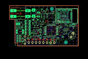
PCB layout
Earlier
PCB layout
Earlier
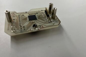
PCB layout
Today
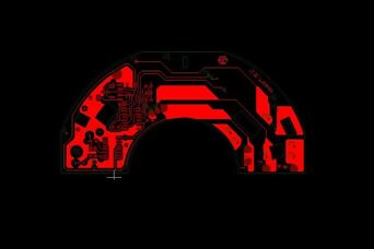
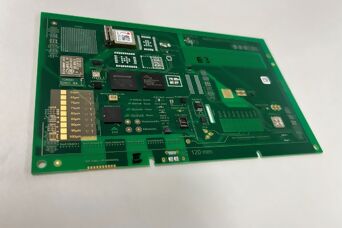
PCB layout
Today
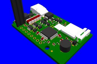
PCB layout
Today
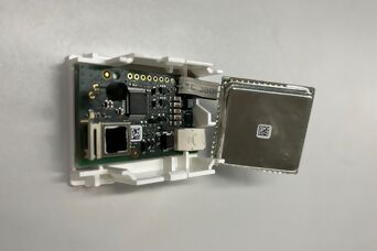
PCB layout
Today
Nowadays, creating a layout is more complex in many respects; it is no longer just a matter of placing components and drawing conductors. The requirements for an electronic device have also changed over time and with them the demands on a PCB layout and equally on the PCB designer in its realisation.

Expertise and interdisciplinary collaboration
The role of the PCB designer has changed along with the requirements for a PCB layout - it is complex, interesting and varied. Sophisticated layout programmes, complex electronic hardware and rapidly evolving trends require a great deal of specialist knowledge. Further training is therefore a core task.
Success factors for successful product development, from electronics development to PCB production, include close cooperation and constructive dialogue with various internal and external specialist departments.
Click on the orange dots to get an overview of the interfaces to the individual departments.


Electronics development
Close cooperation with electronics development is the first milestone in creating a layout. Here, topics such as EMC, temperature resistance, currents, placement, technology, etc. should be taken into account right from the start. Likewise, the right choice of components, and if necessary already a procurement solution for the most important components. For sample or prototype production, the PCB-Designer supports the PCB assembly and procurement of components.
Housing design
The size and space conditions of the PCB in an enclosure require close consultation between enclosure design and PCB-Designer, the eternal «chicken-and-egg» discussion between beautiful design of the enclosure and the inner workings of the final product should be avoided here. Usually, the milestone space estimate helps in advance. If the enclosure is already specified, it can sometimes be difficult to create a functioning layout; often millimetre changes in the design or small replacements of buttons solve a problem. Through regular technical exchange, precisely these problems can be solved together at the outset.
Test equipment construction
To ensure that the assembled PCB can also be tested, a test device is needed. At STEINEL, we have our own InCircuitTest department and a Functional Test department. To build a test device, it is imperative that the PCB-Designer and the test device department work together. The placement of the test points, catch holes, etc. on the layout must be coordinated with the test equipment. This coordination step should be done as early as possible.
Purchasing
In the area of PCB-Procurement, the PCB-Designer supports the purchasing department with technical aspects in the choice of PCB and PCB-Manufacturer, because in terms of quality, manufacturers sometimes differ enormously. Finding the right PCB-Manufacturer for a product is not easy and for certain layouts, once more complex specifications of a PCB have become standard. Technical queries from the manufacturer are usually answered directly by the PCB-Designer and feasibilities of PCB-Production related to the complex layout are discussed with the manufacturer.
Technical office
The PCB-Designer works together with the technical office on various topics. This may be in the preparation of a quotation for a customer, whereby, for example, the production benefit is estimated in order to calculate the lead time, the checking of an SAP parts list for the assembly and mounting of the PCB, or the maintenance of existing products.
Project Management
The close cooperation with the project manager makes it possible to keep to the schedule and ensure that it does not get out of joint due to a PCB that is delivered too late. In the same way, the PCB-Designer is involved in the communication with the customer when certain changes in the layout are planned, or when suggestions for solutions are required as to how the design of the product can be implemented more cheaply, more simply or more conveniently for production.
Incoming goods
In order to ensure that received PCBs have been delivered correctly, the PCB-Designer supports the incoming goods department in checking the correctness and quality of the delivered PCBs.
Production
Early cooperation in the development of a PCB-Layout with production is absolutely central, regardless of whether the PCB is later processed in SMD or THT production. The implemented designs must first and foremost be producible. Therefore, it is of high importance to discuss with the production the possibilities of a placement machine, solderability of the component, quality of the PCB, spacing of components and much more. For later series production, the PCB-Designer provides the necessary data for the placement machines, SPI, AOI and manual placement.
Electronics Laboratory
Electronics development usually needs a sample PCB very quickly at the start in order to test the circuit developed. To speed up this process, prototypes are assembled in-house at STEINEL in small quantities and tested in the company's own EMC laboratory. The electronics lab and the PCB-Designer work together on solutions and optimisations for a functional, producible PCB-Design.
Quality Management
If there are production problems on the basis of printed circuit boards or the assembly of electronic components, the PCB-Designer is involved in the joint solution-finding process between the specialist departments. The PCB designer also provides specialist support to the quality department in the analysis of incorrectly delivered PCBs.
Sales
Through the cooperation between sales and PCB-Designer, any special customer requirements can be assessed in advance and thus certain misunderstandings can be prevented for the preparation of a guideline quotation. The PCB designer also provides technical support here for PCB-specific questions.
Customers
In most cases, open questions from the customer are answered by the customer-facing contact persons in sales, project management or the technical office. If the questions are more technical, the electronics development department and the PCB-Designer are available to clarify the open points directly with the customer. In certain projects, the PCB-Designer even works very intensively with the customer.
The many interfaces show this: At STEINEL, the PCB designer is not ‘just’ a layout designer, but also a team player, solution finder, coordinator, reviewer, listener and supporter for the various specialist departments. Everything revolves around the printed circuit board to create a successful product.

‘Our customised OEM products and projects challenge me time and again and make my job varied, because it's my job to dutifully implement all rules and standards and create a functional PCB design so that the PCB is suitable for production and the product is a success - in an interface function.’